Laser Applications for Electronics & Semiconductors
Semiconductors are the foundation of modern electronic devices and their manufacturing
demands extreme precision, cleanliness and process stability. As device sizes continue to
shrink and functional complexity increases, manufacturers require processes capable of
delivering micron-level accuracy, high repeatability and contamination-free operation.
Laser technology plays a critical role in electronics and semiconductor manufacturing due to
its thin, precise and highly controllable energy delivery. Laser-based processes are widely
used for cutting, marking, coating removal and welding, enabling manufacturers to process
delicate and complex components without physical contact, tool wear or deformation.
Laser processing has become a core enabling technology in semiconductor production,
offering digitally controlled, non-contact operation that supports high-throughput
manufacturing while meeting strict quality, reliability and yield requirements.
Light Mechanics delivers application-driven laser solutions tailored for electronics and
semiconductor manufacturing, supporting scalable production and consistent high-yield
performance across advanced electronic and semiconductor applications.
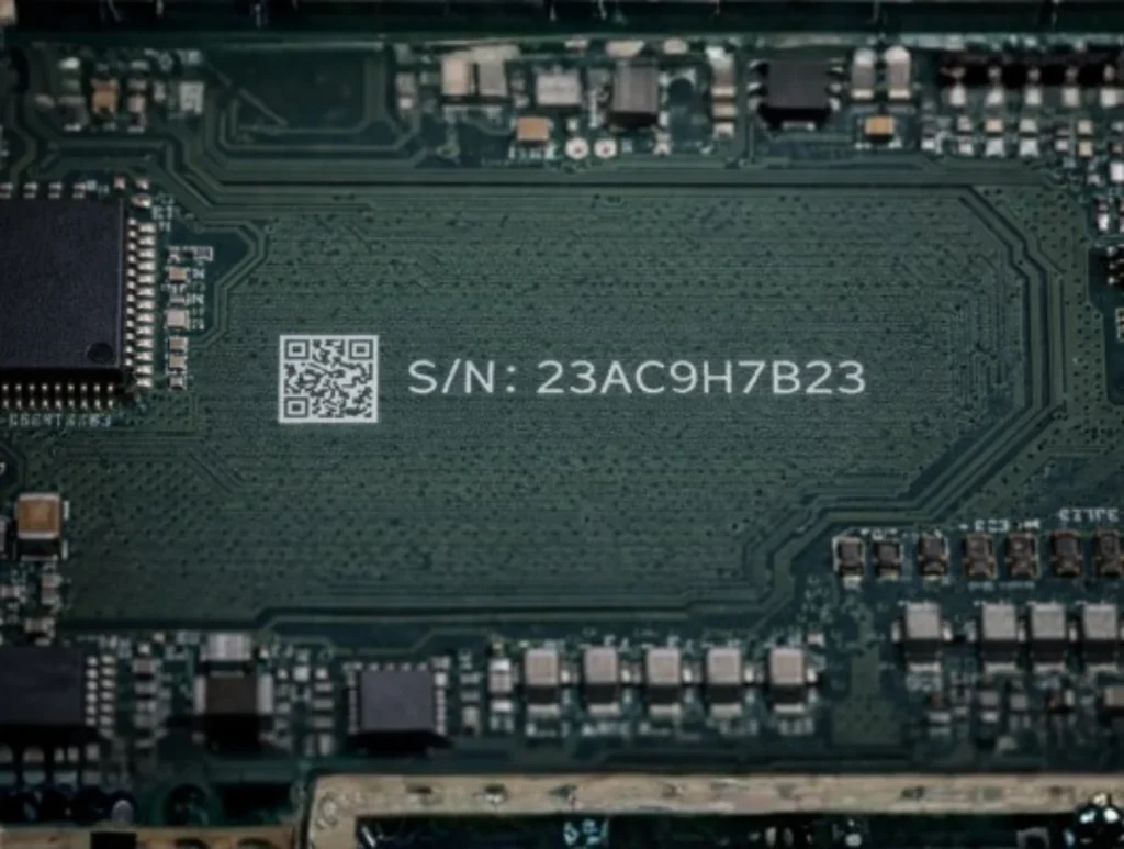
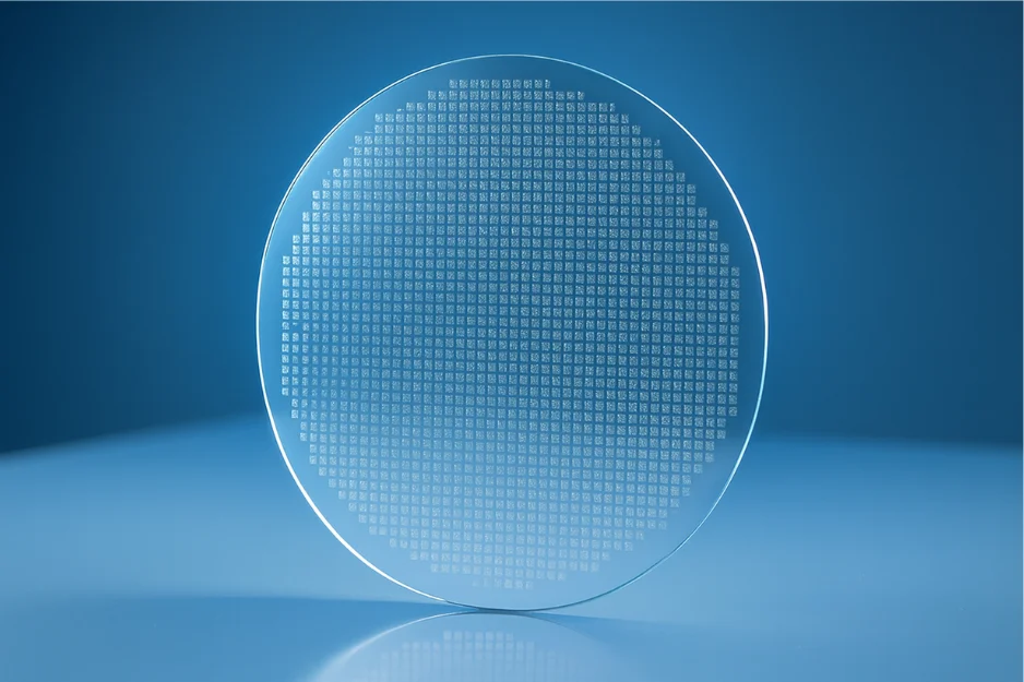
PCB & Wafer Laser Marking
Application Demand
Printed circuit boards and semiconductor wafers require permanent, high-resolution
identification for traceability, quality control and process tracking. Markings must be legible
at micro-scale, applied without physical contact and must not damage sensitive circuits,
layers or device structures.
What Laser Enables
Laser marking enables precise, permanent and non-contact identification directly on PCBs
and wafers with fine spot sizes, stable pulse energy and no mechanical stress. It supports
high-density data matrix codes, serial numbers and logos with excellent contrast while
preserving electrical integrity. The process is fast, repeatable and fully compatible with inline
semiconductor and electronics production.
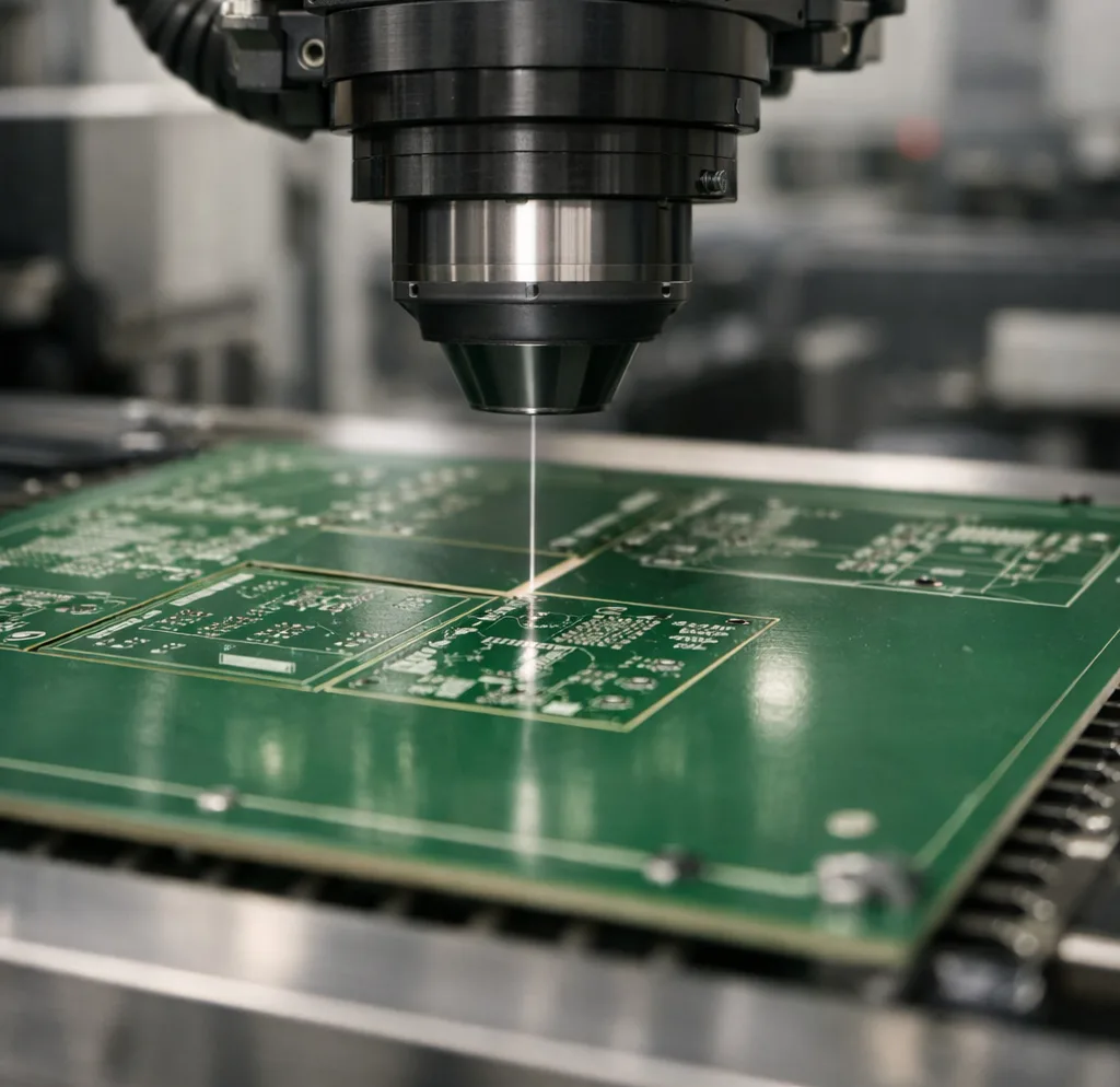
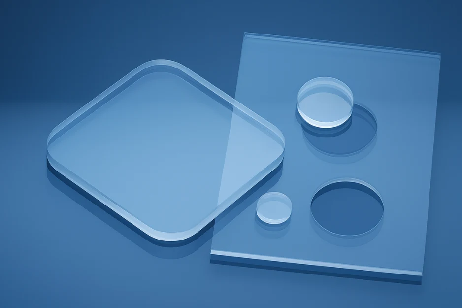
PCB and Wafer Cutting
Application Demand
Printed circuit boards and semiconductor wafers require high-precision separation without
inducing burrs, mechanical stress or micro-cracks that can reduce yield and long-term
reliability. As substrates become thinner and more complex, cutting processes must protect
micro-scale features, multilayer structures and edge integrity.
What Laser Enables
Laser cutting provides clean, burr-free and non-contact separation of PCBs and wafers with
controlled energy input and minimal heat-affected zones. The process prevents mechanical
stress and micro-cracking, ensuring consistent edge quality, improved yield and compatibility
with automated, high-volume electronics and semiconductor production.
Wafer Scribing and Dicing
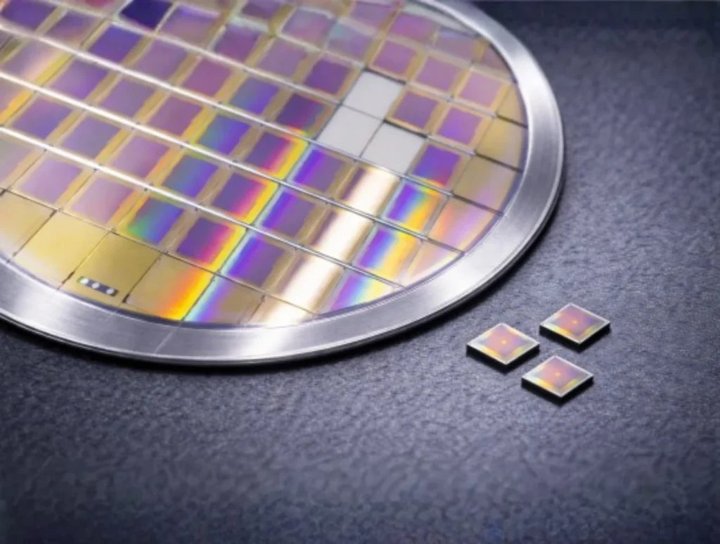
Application Demand
Semiconductor wafers require precise and controlled singulation to produce individual dies
without chipping, cracking or edge damage. As device dimensions shrink and packaging
technologies advance, maintaining die strength, yield and edge quality becomes increasingly
critical.
What Laser Enables
Ultrashort and solid-state lasers enables narrow kerf widths and clean, well-defined scribe
lines with minimal thermal impact on surrounding material. The process reduces chipping,
improves die strength and supports high-yield singulation for advanced semiconductor and
microelectronics packaging.
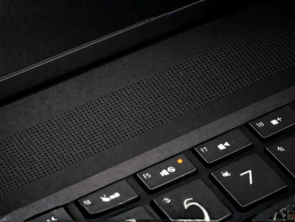
Notebook Audio Hole Drilling
Application Demand
Speaker and microphone openings in notebooks and consumer electronics require precisely
sized and uniformly distributed micro-holes to ensure consistent acoustic performance and
high cosmetic quality. Hole geometry, edge quality and repeatability are critical, as
inconsistencies can affect sound output, appearance and assembly yield.
What Laser Enables
Laser drilling enables highly controlled micro-hole formation with precise diameter and taper
control and burr-free edges. The non-contact process ensures excellent repeatability, clean
aesthetics and consistent acoustic performance while supporting high-speed, automated
production for consumer electronics.
Glass Cutting for Consumer Electronics
Application Demand
Across consumer electronics, optics, automotive and advanced packaging, glass has become a critical material due to its flatness, thermal stability, chemical resistance and optical performance. From cover glass, camera windows, UTG ultra thin substrates and LCD panels to packaging wafers, interposers and rearview mirrors, manufacturers require precise, high throughput processing with tight tolerances. As devices become thinner, coated and more complex, traditional mechanical methods struggle to meet requirements for defect free edges, crack free vias and scalable production.
What Laser Enables
Ultrashort pulse laser technology provides non contact, selective and damage free processing of brittle materials. It enables cutting, drilling and structuring with superior edge quality, minimal thermal impact and repeatable results – even on chemically strengthened or coated substrates. Lasers support complex contours, free form designs and ultra thin glass processing, while reducing particle generation. Optimized material flow in laser systems allows manufacturers to scale efficiently from small batches to mass production, reducing per-component costs while meeting the stringent demands of modern electronics packaging.
Why Choose Light Mechanics
Light Mechanics delivers precision laser machines specifically engineered for electronics and
semiconductor manufacturing. Our systems provide micron-level accuracy, high
repeatability and non-contact processing, ensuring zero-defect production and protection of
delicate components.
With expertise in PCB and wafer marking, cutting, scribing, dicing and micro-drilling, we
enable high-throughput, automated production while maintaining edge integrity, device
reliability and process consistency. Our solutions minimize thermal impact, eliminate
consumables and support inline, scalable manufacturing, helping electronics and
semiconductor manufacturers achieve superior yield, traceability and quality compliance in
increasingly complex, miniaturized devices.